GaN and SiC Power Device Presentations at APEC
04/22/2015 //
In mid-March the Power Sources Manufacturers Association (PSMA) held its annual Applied Power Electronics Conference (APEC), this time in Charlotte, North Carolina, marking the conference’s 30th anniversary.
Considerable attention in the power industry has centered on the emergence of wide bandgap (WBG) material – gallium nitride (GaN) and silicon carbide (SiC) – for use in power devices. Bandgap is the energy required for an electron to jump from the top of the valence band to the bottom of the conduction band within a semiconductor. Put more simply, it is the amount of energy needed to free an electron so that it can become mobile.
At APEC an industry session titled, "Latest Advances in Power Semiconductors, a Less Biased Discussion," focused on the use of WBG components in power devices. WBG materials are interesting in these applications primarily because of their ability to operate at higher temperatures, higher power densities, higher voltages, and higher frequencies than traditional silicon.
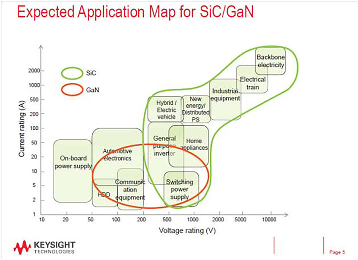
According to Yole Développement analysts (presenting "Market & Technology Trends in Wide BandGap Power Packaging"), WBG technologies SiC and GaN are now almost ready to be implemented in numerous power electronics applications and there is room for each: high voltage and high temperature applications for SiC and low and medium voltage applications for GaN (and especially GaN HEMT transistors). Yole predicts: 1) SiC will stay the preferred choice for high temperature application--SiC diodes are already in production, mainly coupled with IGBT technology; 2) GaN could possibly reach high-voltage values but this will require bulk-GaN as the substrate; and 3) Silicon cannot compete in the high-frequency range.
Yole’s Dr. Pierric Gueguen suggested that WBG market shares will depend on when integrators get benefits from such solutions given that they require additional research expenses at the power module packaging level. Such costs must be compensated for by added value to the system, compared to existing silicon solutions. He explained that the necessary added value would come from integrating WBG devices at higher operating frequencies and temperatures.
The consulting firm also has identified several challenges due to technical requirements. One potential bottleneck for WBG technologies’ adoption is at the power module packaging level. Potential issues include:
- The power module with baseplate is the standard design (70% to 80% of available power modules). DBC (Direct Bond Copper) packaging is the most widespread packaging. These modules are however both complex and expensive.
- Common failure in a power module is caused by thermal cycling. Mismatching CTE (coefficient of thermal expansion) can make layers detach from one another. Some gel filling also cannot handle high temperatures.
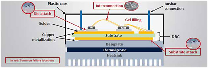
Yole sees improvements in packaging coming from three different places:
- Die interconnection, which is searching for innovative wire bonding or no-wires connection for better lifetime and reliability characteristics;
- Die attach, using new materials for better lifetime; and
- DBC+baseplate, which uses new materials and suppress layers for improved cooling and smaller size
"Wide Band Gap Power Device Evaluation Challenges and Technologies" was presented by Ryo Takeda, Senior Product Planner for Keysight Technologies International. He reiterated that SiC was suitable for very high power (high current/high voltage) application while GaN was suitable for middle range power application.
He said critical evaluation Items for SiC/GaN include:
High Current. Takeda noted that Ron becomes smaller and therefore high current is mandatory for accurate Ron evaluation. Ron also is important to calculate conduction loss.
High Voltage (especially important, Takeda noted, for SiC). This, Takeda said, was a basic parameter but one of the most important parameters from a reliability perspective.
Temperature dependency (also especially important for SiC). Various power electronics products, he pointed out, are used in harsh environments.
Capacitance (Ciss, Coss, Crss, Rg, Normally-on device). Takeda said this was especially important for GaN and noted these were critical parameters for switching performance and important to estimate power losses such as output capacitance loss, etc.
Gate Charge, which was characterized as a critical parameter for switching performance and gate drive circuit design and important to estimate switching loss.
Reliability. Long term reliability is one of the main concerns when adopting new/emerging devices, Takeda said.
Among the challenges in SiC/GaN device evaluation Takeda cited:
Lack of a Standard Solution
How many hours have you invested in isolating your test problems?
Device manufacturers suffer the lack of reference measurement equipment.
Device users have no easy way to make an accurate device evaluation.
High Voltage / High Current
Accuracy is questionable without having a well thought out test circuit and NIST traceable standard.
Temperature dependency
Long cable extension from test equipment to thermostatic chamber results in 1) current reduction, 2) oscillation, and 3) deteriorated accuracy.
Capacitance (Ciss, Coss, Crss, Rg & Normally-on)
Complicated connections and special techniques result in measurement problems.
Gate Charge
It is difficult to construct a test system with good accuracy and safety, he said.
Intuitive and Standard User Interface
"Anybody" should be able to conduct device evaluation without training.
Ranbir Singh of GeneSiC Semiconductor next presented "Silicon Carbide Switches in Emerging Applications".
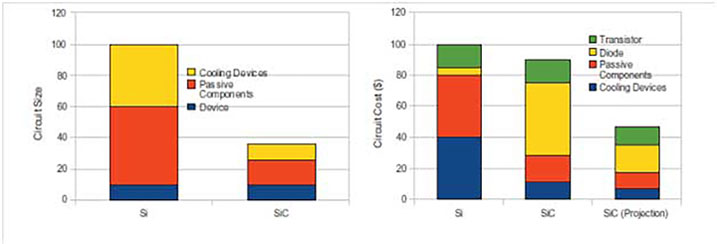
Example of a DC-DC converter circuit (Si vs. SiC) at relevant voltage levels
Among the key SiC application trends Singh reported on were:
Solar Inverters with 1000-1500 VDC bus architectures. He said the solar industry is trending toward higher power ratings, since inverter cost per watt decreases with inverter power. The industry is also trending to higher system voltages in order to reduce wire costs (smaller cross-section cables, fewer generator connection boxes, less cabling) and power losses. On the DC side, he said most large terrestrial PV systems currently operate with a DC voltage of 1000 V with 1500 V DC operation coming soon. For handling a DC link voltage of 1500 V, 1200 V power transistors are required in a three-level topology, and 3300 V power transistors for a two-level topology.
In a typical boost stage, a 200 to 400 V DC solar panel input is boosted to an output voltage of 1000 V DC (or 1500 V DC). Singh pointed out that the power electronics design engineer’s goal is to keep the system efficiency as high as possible, but at the same time minimizing cost through size, weight and component reduction. The high-efficiency switching properties of SiC power semiconductor devices are attractive for the DC-DC boost stage in a PV system because: 1) high power density coupled with high frequency operation results in lower overall converter balance-of-system (BOS) costs; 2) higher blocking voltage (1200-1700 V) SiC transistors enable lower component count, more compact circuit topologies and controls and 3) the SiC parts run cooler than their Si counterparts, which reduces the cooling requirements.
Data Centers with 380 V DC architectures. According to Singh more than 50% of electric power is wasted for power conversion, distribution, emergent power back-up, and temperature cooling within a large scale data center. Recently, however, high-voltage (380 V DC) distribution has become popular since it offers increased efficiency, reduced cable costs, floor-space savings, and relatively high availability. He said the 800 V DC Link voltage in a 380 V DC distribution scheme would require 1200 V rated power devices and that 1200 V SiC power transistors offer significantly faster switching and higher junction temperatures than Si IGBTs, which can improve circuit efficiency.
Next year APEC 2016 will be held 19 March to 24 March at the Long Beach Convention and Entertainment Center in Long Beach, CA.
Murray Slovick

Murray Slovick is Editorial Director of Intelligent TechContent, an editorial services company that produces technical articles, white papers and social media posts for clients in the semiconductor/electronic design industry. Trained as an engineer, he has more than 20 years of experience as chief editor of award-winning publications covering various aspects of consumer electronics and semiconductor technology. He previously was Editorial Director at Hearst Business Media where he was responsible for the online and print content of Electronic Products, among other properties in the U.S. and China. He has also served as Executive Editor at CMP’s eeProductCenter and spent a decade as editor-in-chief of the IEEE flagship publication Spectrum.